Laser ablation is rapidly becoming a preferred method for processing silicone. This is because of its high precision and flexibility. In this article, we will discuss its principle, key parameters, and its growing use in industries such as electronics, healthcare, and manufacturing.
What Is Silicone Laser Ablation?
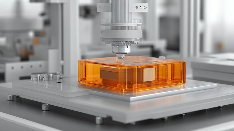
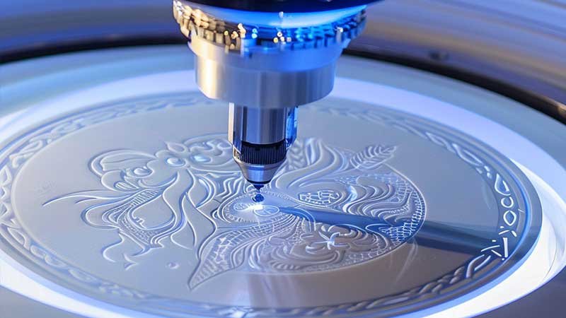
Silicone Laser Ablation is an advanced technology that uses a high-energy laser beam to precisely remove or modify the surface of silicone. By adjusting the laser’s energy, wavelength, and pulse, it can create fine structures like holes, grooves, and patterns at the micron or nanometer scale.
This process carves details much finer than a human hair without causing the silicone to melt or deform. It is used in high-tech products such as smartwatches, medical chips, and electric vehicle battery seals.
What Is the Principle of Silicone Laser Ablation?
When a high-energy laser beam hits the silicone surface, the material absorbs the laser energy and quickly converts it into heat. If the temperature in a localized area exceeds the threshold for vaporization or decomposition, the silicone rapidly turns into gas or small particles that are removed.
For specific laser wavelengths, photochemical reactions may also occur, directly breaking down the silicone’s molecular chains and aiding its decomposition.
By precisely controlling the laser’s power, pulse, and scanning path, it is possible to remove material from the silicone surface with micron or even nanometer precision, creating the desired patterns, markings, or microstructures.
What Are the Key Parameters in Silicone Laser Ablation?
| Parameter | Typical Range/Options | Meaning and Impact |
| Laser Wavelength | 355nm (UV) / 10.6μm (CO₂) | Determines material absorption and processing precision. UV is suitable for fine structures, while CO₂ is good for fast coarse processing. |
| Laser Power | 10-200W | Higher power increases ablation depth, but power >150W may cause carbonization. |
| Pulse Frequency | 1-200kHz | High frequency (>50kHz) improves surface quality, while low frequency (<20kHz) increases single pulse energy, suitable for deep hole processing. |
| Scanning Speed | 100-2000mm/s | Faster speeds reduce thermal impact but must match with power (higher power → faster speed). |
| Focus Offset | ±0.1mm | Positive offset (expanded spot) reduces energy density. Negative offset (compressed spot) enhances penetration. |
| Gas Environment | Air / Nitrogen / Argon | Nitrogen reduces oxidation and carbonization, while Argon reduces plasma shielding effects, improving energy efficiency by 20%. |
| Repetition Count | 1-10 times | Multiple scans control depth (adding 20-50μm per scan), but care is needed to avoid sidewall melting. |
| Cooling Method | Natural cooling / Water-cooled substrate / Liquid nitrogen spray | Liquid nitrogen cooling (-196°C) can reduce thermal impact zone (HAZ) from 50μm to 10μm, but adds 30% cost. |
Laser Wavelength Selection
Medical-grade Silicone: It is recommended to use a 355nm UV laser. Its high photon energy (3.5eV) can break Si-O bonds directly, enabling no thermal damage processing (Ra < 1μm). This is especially useful for medical-grade silicone where precision is critical.
Industrial-grade Silicone: 10.6μm CO₂ laser is suitable for faster ablation due to its thermal effects (efficiency up to 5cm²/min). However, post-processing is necessary to remove the carbonized layer formed during the ablation process. This wavelength is typically used for industrial applications where speed is prioritized over precision.
Power-Speed Coordination
Golden Formula: Ablation depth ≈ (Power × √Frequency) / Speed
Example: 100W laser at 50kHz, 500mm/s gives an ablation depth of approximately 80μm.
Safety Threshold: Power density >10⁷ W/cm² may cause material breakdown.
Pulse Frequency and Edge Quality
High Frequency (>100kHz): The pulse interval is less than 10μs. This reduces heat accumulation and is ideal for processing bio-mimetic channels, where edge roughness is kept below Ra < 2μm.
Low Frequency (<20kHz): The single pulse energy is greater than 1mJ, making it suitable for processing battery seal slots. This frequency ensures consistent depth, with a tolerance of ±5μm, providing reliable results for deeper and more intricate cuts.
Gas Environment Optimization
Nitrogen Purge: With a flow rate of 15-20L/min, carbon residue is reduced by 60%, making it suitable for food-grade silicone processing.
Argon Protection: When processing conductive silicone, Argon prevents metal filler oxidation (resistance variation rate < 3%).
Cooling Strategy Comparison
| Cooling Method | Thermal Impact Zone (HAZ) | Cost Increase | Application |
| Natural Cooling | 50-100μm | 0% | Low-precision decorative patterns |
| Water-Cooled Substrate | 30-50μm | 15% | Medium-precision industrial components |
| Liquid Nitrogen Spray | 10-20μm | 30% | Medical device microstructures |
Typical Parameter Combination Cases
Medical Microfluidic Chip
- Parameters: 355nm, 80W, 150kHz, 800mm/s, Nitrogen, 3 scans, Liquid Nitrogen cooling
- Result: A 50μm wide x 150μm deep channel is fabricated with sidewall verticality greater than 89°, and no carbon residue remains.
New Energy Vehicle Sealing Pad
- Parameters: 10.6μm, 150W, 20kHz, 300mm/s, Air, 1 scan, Natural cooling
- Result: A 200μm wide x 500μm deep trapezoidal groove is etched with a processing speed of 12 parts per minute.
Flexible Electronics Insulating Grooves
- Parameters: 355nm, 50W, 100kHz, 1200mm/s, Argon, 5 scans, Water-cooled substrate
- Result: An 80μm wide groove is etched on conductive silicone with a dielectric strength greater than 20kV/mm.
What Other Factors Influence the Laser Ablation Process of Silicone?
In addition to the laser processing parameters, the inherent properties of silicone play a crucial role in influencing the final results of laser ablation.
| Factor | Impact on Laser Ablation |
| Silicone Type & Formulation | Laser absorption, thermal conductivity, and decomposition properties |
| Hardness | Crack, peel, melt or deform |
| Surface Condition | Uneven ablation and uneven energy distribution |
Firstly, the type of silicone and its formulation are the primary factors. Different types of silicone have differences in molecular structure and crosslinking density. These differences directly affect their ability to absorb specific laser wavelengths, thermal conductivity, and decomposition characteristics at high temperatures. Besides, fillers and pigments can significantly alter the optical absorption, heat capacity, and thermal conductivity of the material. This, in turn, influences laser energy absorption efficiency, ablation threshold, and material removal rate.
Next, the hardness of silicone also impacts the laser ablation process. Harder silicone may be more prone to brittle fracture or peeling under laser exposure, while softer silicone is more likely to melt or deform. Hardness also affects the efficiency of removing ablation products and the final surface finish.
Finally, the surface condition of silicone, such as its cleanliness and initial roughness, should not be overlooked. Contaminants like oil or dust on the surface may absorb or scatter laser energy, reducing the efficiency of energy transfer to the silicone surface and potentially leading to uneven ablation. A rough surface can also cause uneven distribution of laser energy, affecting the uniformity and precision of the ablation.
Therefore, before performing silicone laser ablation, it is essential to fully understand and evaluate the inherent properties of silicone. Optimizing the laser process parameters based on these characteristics is a key step to achieving the desired ablation results.
What Are the Applications of Silicone Laser Ablation?
Silicone laser ablation has shown great potential across multiple fields.
| Field | Applications |
| Microprocessing & Microstructure Manufacturing | 3D fluid circuits, cell culture chips, micro-lenses, flexible electronics, sensors, non-slip surfaces |
| Surface Modification | Optical devices, SiO2 film |
| Biomedical Applications | Photosensitizers, antibacterial agents, medical devices, catheters |
| Industrial Applications | Silicone molds, carbon fiber-reinforced silicone composites |
Microprocessing and Microstructure Manufacturing
Laser ablation is used to create tiny holes, like 1 µm diameter through-holes. It is ideal for applications such as 3D fluid circuits or cell culture chips. Besides, 157 nm F2 laser ablation can form SiO2 micro-protrusions on silicone surfaces, which are then processed into micro-lenses with focal lengths between 10-170 µm. Laser ablation is also widely used for surface patterning in flexible electronics, sensors, or non-slip surfaces.
Surface Modification
A 193 nm ArF laser can modify the silicone surface to create a silica-like structure, producing white light luminescence. This is useful in optical devices. Furthermore, high-energy ablation combined with an oxygen atmosphere allows for the deposition of a transparent SiO2 film on a substrate, achieving a 95% transmittance rate.
Biomedical Applications
Femtosecond lasers can be used in water to ablate silicone and produce uncontaminated silicone nanoparticles. These nanoparticles can be used as photosensitizers or antibacterial agents. In medical device manufacturing, laser ablation can microstructure catheter surfaces, enhancing biocompatibility or drug-release performance.
Industrial Applications
Laser ablation is employed to clean residues from silicone molds in a non-contact and chemical-free manner. It is also used in composite material processing, such as precise cutting or surface treatment of carbon fiber-reinforced silicone composites.
Why Silicone Laser Ablation Is Better Than Traditional Engraving Methods?
Silicone laser ablation offers several advantages over traditional engraving methods. Its non-contact nature prevents material deformation and damage, making it especially suitable for soft silicone. The high precision of the laser allows for micron-level processing, which surpasses traditional mechanical engraving. Besides, laser ablation provides great flexibility, as complex patterns can be easily customized through software without the need to change molds. It can also achieve surface modifications, adding new properties to the silicone. Moreover, it is easy to automate, which could reduce maintenance costs in the long run. These benefits make laser ablation a more powerful and promising method for silicone processing.
Conclusion
Silicone laser ablation brings a host of advantages over traditional methods, offering precision, flexibility, and the ability to modify silicone surfaces without causing damage. As technology advances, its potential for even more industries is vast. Embrace this innovation to unlock new possibilities in silicone processing.
With years of expertise in silicone manufacturing, we specialize in delivering high-quality silicone products using advanced production techniques. Whether you need custom designs or specific features, our team is here to bring your vision to life. Get in touch with us today to create the perfect silicone solution tailored to your needs.